SuVolta, which helps chip makers overhaul their semiconductor designs so they use less power, has raised $10.6 million in a new round of funding.
The Los Gatos, Calif.-based company has now raised $50.4 million since 2009. That’s a lot of money, and it tells you that it’s no small task to create a new chip technology these days. But it also speaks to the potential of SuVolta, which is trying to reduce power consumption in a wide range of chips by 50 percent. That kind of technological advance will enable chip makers to cram more powerful electronics into smartphones and tablets while extending battery life at the same time.
New investor Fujitsu Semiconductor participated in the round along with existing investors Kleiner, Perkins, Caufield, and Byers (KPCB), August Capital, New Enterprise Associates (NEA), Northgate Capital, and DAG Ventures. SuVolta will use the money to accelerate the integration of its technology into chip designs. Fujitsu is the first major licensee for SuVolta’s technology.
“As we move toward an increasingly connected world, reducing power consumption and controlling costs are the semiconductor industry’s greatest challenges,” said Forest Baskett, a SuVolta board member and general partner at NEA. “SuVolta is solving these challenges while enhancing the industry’s most cost-effective process technology — planar, bulk CMOS [complementary metal-oxide-semiconductor] — which is critical for the emerging Internet of things market.”
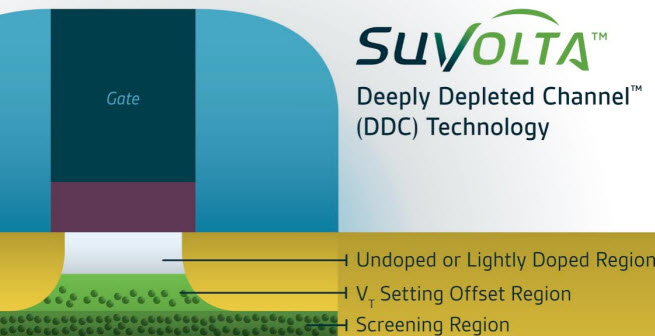
SuVolta calls its technology Deeply Depleted Channel, a refashioning of the transistor, the basic building block of electronic devices. SuVolta and rivals like Intel are working on ways to extend Moore’s Law, the notion put forth in 1965 by Intel chairman emeritus Gordon Moore that the number of transistors on a chip will double every two years. Japan’s Fujitsu is in full production with SuVolta’s technology.
SuVolta attacks a problem called transistor variation. It minimizes the electrical variation in each of the millions of transistors on a chip. On the manufacturing level, SuVolta merely tweaks the “recipe” for making a chip. The result is that it reduces the variation in voltage for a chip, allowing for efficiency improvements.
Haruyoshi Yagi, the corporate senior executive vice president at Fujitsu Semiconductor, said, “Our investment in SuVolta is a reflection of the excellent working relationship between the companies and our confidence in the value of DDC technology at a variety of process nodes.”
“This funding demonstrates the excitement surrounding our technology and the benefits it can bring large markets such as DRAM, [Internet of things], and mobile computing,” said Bruce McWilliams, the president and CEO of SuVolta. “With DDC technology now in volume production, we are seeing increased interest from leading foundries and semiconductor companies seeking a competitive advantage through ultra-low-power optimization.”
The company has 50 employees.
Related articles


![Reblog this post [with Zemanta]](http://img.zemanta.com/reblog_e.png?x-id=10d472dc-855b-413a-b411-2657d9ec6386)
VentureBeat's mission is to be a digital town square for technical decision-makers to gain knowledge about transformative enterprise technology and transact. Learn More