SuVolta has been promising big gains in power efficiency for chip makers for a long time. Now it’s living up to that promise, announcing today that Fujitsu Semiconductor is now in volume production on a chip that uses SuVolta’s power-saving technology.
Fujitsu is shipping an image processing chip with SuVolta’s Deeply Depleted Channel transistors, which are the on-off switches that are the building blocks of electronic circuits on chips. Fujitsu’s chip has 30 percent lower power consumption and twice the processing performance compared to existing products. For consumers, that means they will get faster, better, cheaper, and more power-efficient gadgets in the future.
The Fujitsu Milbeaut image processor chip represents the culmination of a successful joint development program between the companies. Fujitsu designed SuVolta’s technology into its 65-nanometer and 55-nanometer production facilities, and it has met all production, yield, and reliability requirements. The collaboration was first announced in 2011.
“What SuVolta and Fujitsu Semiconductor have done is significant for the semiconductor industry,” said Handel H Jones, the chief executive at market research firm IBS. “Working together, the companies have essentially implemented a ‘midlife kicker’ to Fujitsu’s 55nm process technology, enabling advances in IC functionality with much less costs and redesign than those required by node migration to 40nm or 28nm. Since the majority of IC manufacturing today is at 90nm to 40nm process nodes, the implication and benefits to the industry are significant.”
“The latest example is MB86S22AA Milbeaut image processor which was made possible by SuVolta’s innovative technology and Fujitsu Semiconductor’s accumulation of expertise in putting process technology into volume production,” said Amane Inoue, corporate senior vice president at Fujitsu Semiconductor in Japan. “By collaborating with SuVolta to bring up ultra-low-power DDC-transistor 65nm and 55nm processes, Fujitsu Semiconductor is not only enabling advancements in our ASIC products, but also will enhance the designs of COT customers.”
“The Milbeaut chip announced today by Fujitsu Semiconductor exemplifies the power-performance advantages of a DDC-enabled process technology, while demonstrating the manufacturability of the DDC technology,” said Bruce McWilliams, president and CEO at SuVolta. “We are delighted with the advances Fujitsu is making utilizing DDC-enabled low-power processes, and we look forward to additional DDC transistor-based products being announced.”
The technology addresses a fundamental problem in the physics behind transistors, the basic building blocks of all electronic chips. The technology could help improve battery life in portable products — smartphones, tablets, and notebooks — and offer an alternative to a revolutionary Intel technology known as Tri-Gate.
Both SuVolta and Intel are working on ways to extend Moore’s Law, the notion put forth in 1965 by Intel chairman emeritus Gordon Moore that the number of transistors on a chip will double every two years. Japan’s Fujitsu is in full production with SuVolta’s technology.
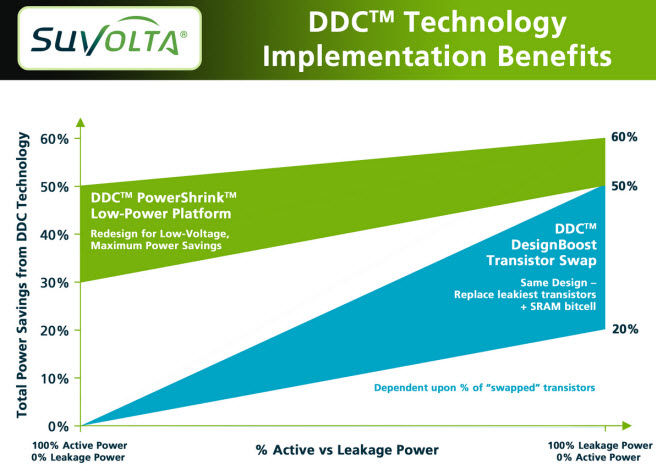
SuVolta attacks a problem called transistor variation. It minimizes the electrical variation in each of the millions of transistors on a chip. On the manufacturing level, SuVolta merely tweaks the “recipe” for making a chip. The result is that it reduces the variation in voltage for a chip, allowing for efficiency improvements.
SuVolta is based in Los Gatos, Calif., has funding from Kleiner Perkins Caufield & Byers, August Capital, NEA, Bright Capital, Northgate Capital and DAG Ventures. The company began life as DSM Technologies in 2006, but went through a reboot in 2009. It has raised $76.5 million to date, but ony $39.8 million of that since 2009.
VentureBeat's mission is to be a digital town square for technical decision-makers to gain knowledge about transformative enterprise technology and transact. Learn More