Apple announced the new iPad Air 2 just last week, and already the good people at iFixit have torn it apart. What they’re looking for: component parts that are designed into the device differently than in previous iterations, and what that means to the “repairability” of the device.
The iFixit teardown experts found a mixed bag with the Air 2.
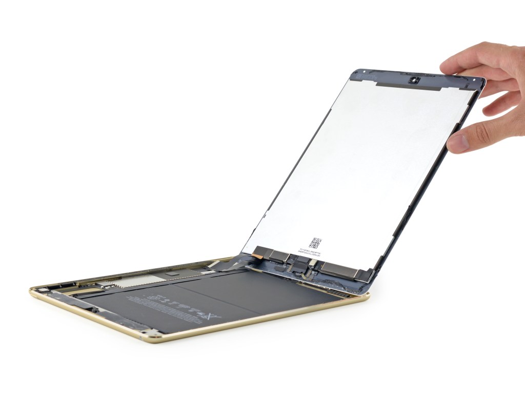
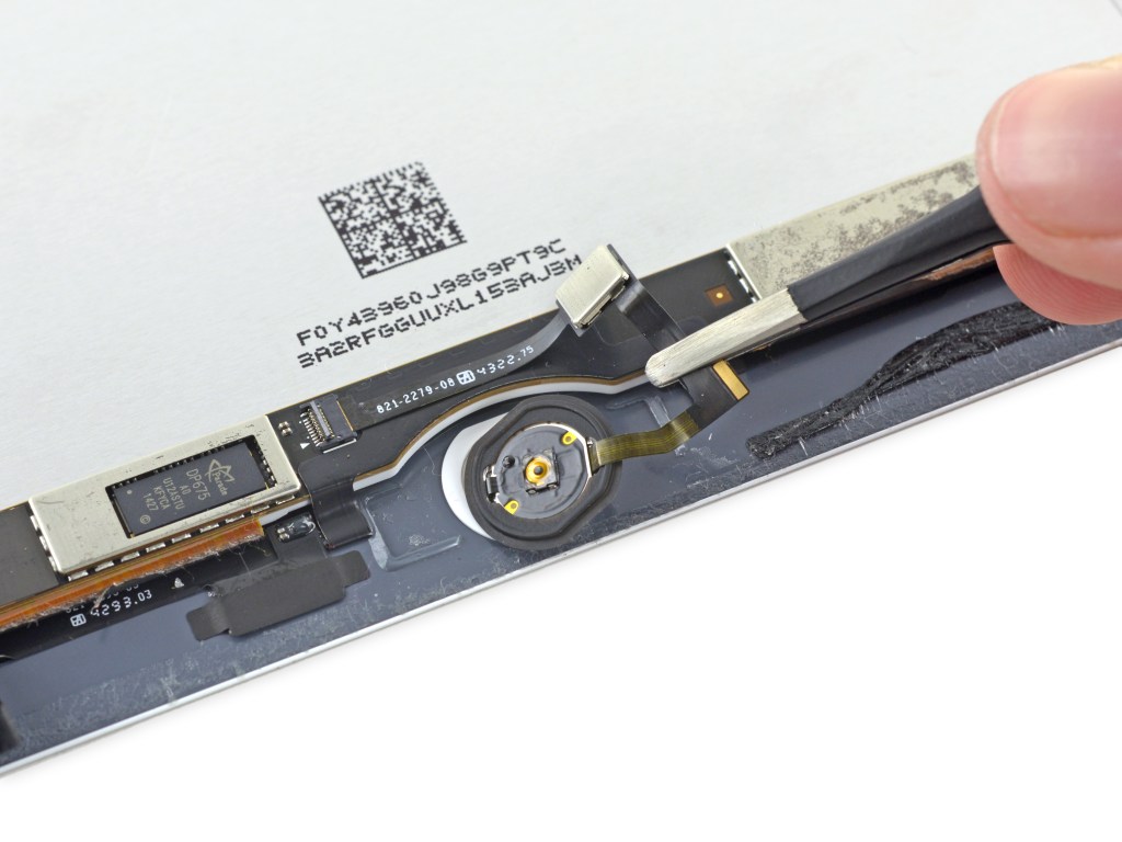
On the plus side, they noted that the wiring is better positioned than in the first iPad Air. “Upon successfully opening the iPad Air 2, we immediately notice that all the display cables now reside near the lower edge,” iFixit writes in its teardown blog. “This is a welcome change from the previous iPad Air, whose digitizer and LCD cables effectively booby-trapped two edges of the display.”
On the other hand, the team found a few important things locked down and hard to remove and repair. “Upon removal of the logic board, we are saddened to see that the Lightning cable remains soldered to the logic board,” iFixit says in the blog. “This makes logic board removal even more of a chore. This also means that replacing the Lightning Connector requires replacing the entire logic board.”
AI Weekly
The must-read newsletter for AI and Big Data industry written by Khari Johnson, Kyle Wiggers, and Seth Colaner.
Included with VentureBeat Insider and VentureBeat VIP memberships.
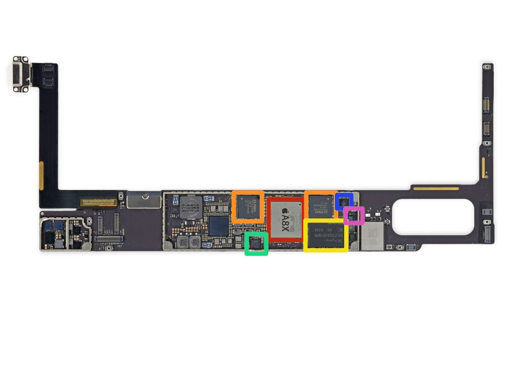
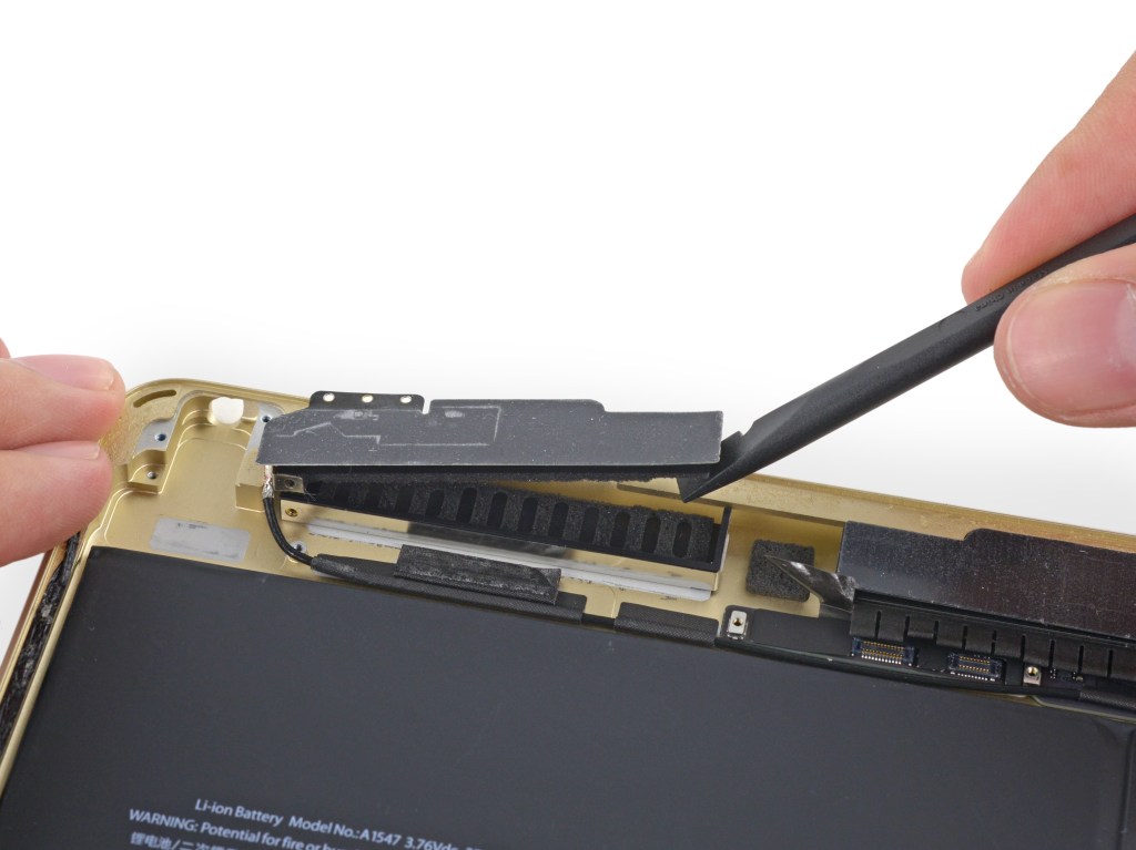
Below are some of the main components of the new Air, as seen from the inside of the device.
You can find iFixit’s full teardown here.

Above: At last, the circuit board . . . RED = Apple APL1012 A8X 64-bit Processor
ORANGE = Elpida (Micron Technology) F8164A3MD (two identical chips)
YELLOW = SK Hynix H2JTDG8UD1BMR 128 Gb (16 GB) NAND Flash
GREEN = NXP 65V10 NFC Module (as found in the iPhone 6 and 6 Plus)
BLUE = Apple (Cirrus Logic) 338S1213 Audio Codec
PURPLE = NXP Semiconductors LPC18B1UK ARM Cortex-M3 Microcontroller (Apple M8 Motion Co-Processor)
VentureBeat's mission is to be a digital town square for technical decision-makers to gain knowledge about transformative enterprise technology and transact. Learn More


