Carbon nanotubes are the leading candidate to replace silicon in semiconductor chips after the decades-long run of silicon electronics runs out. And IBM is hoping to usher along that transition with a new breakthrough being announced today.
In the October 2 issue of the journal Science, IBM researchers say they have overcome one of the most daunting challenges around carbon nanotube transistors, which are the building blocks of electronic circuits with dimensions that are measured in billionths of a meter. Carbon nanotubes may be the best way to uphold Moore’s Law, or the doubling of the number of transistors every couple of years. Moore’s Law is the metronome of the modern age, and it enables constant progress in the $335 billion chip industry.
Carbon nanotube chips could greatly improve the capabilities of high-performance computers, enabling Big Data to be analyzed faster, increasing the power and battery life of mobile devices and the Internet of Things, and allowing cloud data centers to deliver services more efficiently and economically, IBM said.
After decades of progress, the speeds of microprocessors stalled around the early 2000s at 3GHz to 5GHz, mainly because silicon is reaching its physical limits. Carbon nanotubes, by contrast, can operate as transistors (or tiny electrical switches) at dimensions smaller than 10 nanometers, or 10,000 times thinner than a strand of human hair. That’s well below the size of today’s leading silicon technology (14 nanometers).
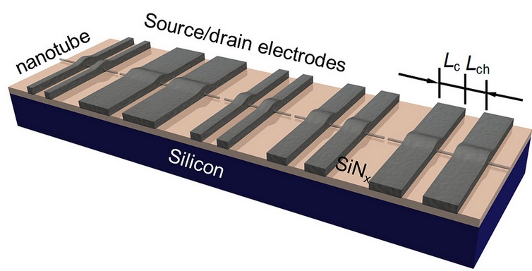
But those nanotubes are like spaghetti, and they have to be marshaled and controlled precisely to function as electronic circuitry. The contact points for the nanotubes create a lot of electrical resistance, which hinders overall performance. IBM has developed a novel way, at the atomic level, to weld — or bond — the metal molybdenum to the ends of carbon nanotubes to create a completely new contact structure.
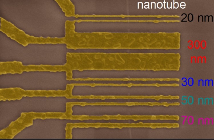
Using this approach, the researchers in Yorktown Heights, N.Y., demonstrated the smallest contacts for carbon nanotubes at 9 nanometers, where the performance did not suffer despite the tiny dimensions. IBM’s carbon nanotube results satisfy the contact requirement all the way up to the 1.8-nanometer node (four technology generations of manufacturing technology away), showing that the technology can scale sooner than the industry thinks, IBM said.
Earlier this summer, IBM unveiled the first 7-nanometer node silicon test chip, pushing the limits of silicon technologies. By investing further in carbon nanotubes to replace traditional silicon, IBM wants to pave the way for a post-silicon future and make good come from its $3 billion investment in research and development.
“These chip innovations are necessary to meet the emerging demands of cloud computing, Internet of Things and Big Data systems,” said Dario Gil, vice president of science and technology at IBM Research, in a statement. “As technology nears the physical limits of silicon, new materials and circuit architectures must be ready to deliver the advanced technologies that will drive the Cognitive Computing era. This breakthrough shows that computer chips made of carbon nanotubes will be able to power systems of the future sooner than the industry expected.”
Carbon nanotubes represent a new class of semiconductor materials that consist of single atomic sheets of carbon rolled up into a tube. The carbon nanotubes form the core of a transistor device whose superior electrical properties promise several generations of technology scaling beyond the physical limits of silicon.
Electrons in carbon transistors can move more easily than in silicon-based devices, and the ultra-thin body of carbon nanotubes provide additional advantages at the atomic scale. Inside a chip, contacts are the valves that control the flow of electrons from metal into the channels of a semiconductor. As transistors shrink in size, electrical resistance increases within the contacts, which impedes performance. Until now, decreasing the size of the contacts on a device caused a commensurate drop in performance — a challenge facing both silicon and carbon nanotube transistor technologies, IBM said.
IBM researchers had to forego traditional contact schemes and invented a metallurgical process akin to microscopic welding that chemically binds the metal atoms to the carbon atoms at the ends of nanotubes. This “end-bonded contact scheme” allows the contacts to be shrunk to below 10 nanometers without the performance of the carbon nanotube devices deteriorating.
“For any advanced transistor technology, the increase in contact resistance due to the decrease in the size of transistors becomes a major performance bottleneck,” said Shu-Jen Han, manager of the nanoscale science and technology group at IBM Research, in a statement. “Our novel approach is to make the contact from the end of the carbon nanotube, which we show does not degrade device performance. This brings us a step closer to the goal of a carbon nanotube technology within the decade.”
VentureBeat's mission is to be a digital town square for technical decision-makers to gain knowledge about transformative enterprise technology and transact. Learn More


