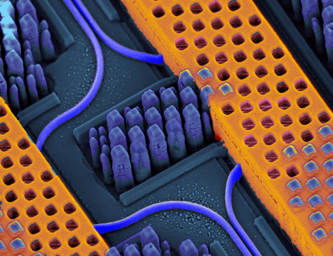
IBM is announcing today it has created breakthrough silicon nanophotonics chips, or those that can use traditional silicon technology and laser light to transfer data at extremely high speeds. These components — silicon and lasers — have been separate in the past, but IBM can now make them side-by-side, combining optical with electrical circuits on the same chip.
The result of this “breakthrough” could unplug the bottleneck in giant data centers and supercomputers, which have been throttled by data traffic jams and high-cost interconnection systems.
After years of research, IBM says it will be able to manufacture these optical chips in standard silicon semiconductor chip factories. That is important, since the problem slowing down computers today isn’t processing or memory, but the interconnections between them that have become bottlenecks. IBM says it can now move the technology from the lab to “fab,” or commercial silicon chip fabrication plants.
AI Weekly
The must-read newsletter for AI and Big Data industry written by Khari Johnson, Kyle Wiggers, and Seth Colaner.
Included with VentureBeat Insider and VentureBeat VIP memberships.
“This technology breakthrough is a result of more than a decade of pioneering research at IBM,” said Dr. John E. Kelly, Senior Vice President and Director of IBM Research. “This allows us to move silicon nanophotonics technology into a real-world manufacturing environment that will have impact across a range of applications.”
Right now, optical components can guide laser light and convert it into electrical signals, which can be processed in silicon chips. But the optical components are bulky and expensive. By embedding the optical components inside the silicon chips, IBM will be able to create data highways that can keep up with the stream of information that has to be processed inside high-speed servers and supercomputers.
“This will help us get past a significant problem in the industry,” said Solomon Assefa, nanophotonics scientist for IBM Research, in an interview with VentureBeat. “When you do a Google search today, it happens inside a big data center, not inside a single chip. The data are stored all over the place, and you have to reach it through fast interconnects.”
The silicon nanophotonics technology can be embedded inside a 90-nanometer chip. Such a chip is easy to make and isn’t as advanced as a state-of-the-art 32-nanometer chip (which has smaller circuitry), but it can be manufactured at low costs and meet performance requirements over the next decade.
Silicon nanophotonics takes advantage of pulses of light for communication, but it is different from other solutions — such as those that Intel has tried to make for years — because it is 100 times smaller.
“We build at the smallest level where these components can direct light,” Assefa said. “the technology is ready for prime time.”
It is just in time for the era of “big data.” Data being created and transmitted over enterprise networks continues to grow due to an explosion of new applications and services. Silicon nanophotonics can enable the industry to keep pace with increasing demands in chip performance and computing power. Today’s optical components have to be chained together in a very expensive solution.
In this era, computers will need to access data that is either a few centimeters or a few kilometers away and move terabytes of data using the light pulses through optical fibers.
IBM began its current approach as a test in 2010. Now it can transfer the technology in a factory, simply by adding a few processing modules into a factory line. The optical components — such as wavelength division multiplexers (WDM), modulators, and detectors — rest side by side with complementary metal oxide semiconductor (CMOS) electrical circuitry (a normal silicon chip).
A single chip could transfer data at 25 gigabits per second, something that requires a chip and a number of expensive optical components today. It can also feed a number of parallel optical data streams into a single optical fiber, or multiplex the streams. That will in turn allow the communications to scale up to delivering terabytes of data between distant computer systems.
Assefa will deliver a presentation on the subject at the IEEE International Electron Devices Meeting (IEDM) in San Francisco this week.
VentureBeat's mission is to be a digital town square for technical decision-makers to gain knowledge about transformative enterprise technology and transact. Learn More