 Fujitsu revealed today that it has confirmed that startup SuVolta’s PowerShrink technology can cut power consumption in a chip by 50 percent without hurting performance.
Fujitsu Semiconductor, a division of the big Japanese electronics giant, is making the announcement today at the International Electron Devices Meeting for chip designers in Washington D.C.
When coupled with other techniques for lowering voltage, the technology can reduce power consumption by 80 percent or more. That’s a fundamental breakthrough, and it’s a rare one, since most venture investments go into applications these days, not core technology.
It’s also an incredibly significant breakthrough that challenges the giants of microprocessor manufacturing, Intel, AMD and Nvidia. Reducing power consumption is the biggest challenge in electronics today, since it means mobile devices can last longer on a battery charge. Once it hits the market in 2012, the technology could enable much smaller, thinner and more powerful laptops, smartphones, and tablets.
Los Gatos, Calif.-based SuVolta, which came out of stealth mode in June, also disclosed the first details of how its low-power transistor technology, dubbed Deeply Depleted Channel (DDC), works. The technology will allow for better low-power chips for at least the next couple of generations through sub-20-nanometer production. (A nanometer is a billionth of a meter.)
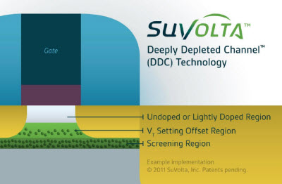
The DDC transistor (pictured in the graphic below) reduces threshold voltage variability and enables continued shrinkage of chip circuits. The structure on a transistor works by forming a deeply depleted channel when a voltage is applied to the transistor. Fujitsu has been able to use the technology in a test memory chip known as an static random access memory (SRAM), which can operate below 500 millivolts with the SuVolta technology. In that test chip, voltage was reduced two-fold and the signal-noise ratio was improved two-fold.
If it works across all sorts of chips, it could extend battery life on one end of the computing spectrum and reduce the spiraling electrical costs for servers and supercomputers.
 The DDC has different regions that allow for different levels of flow of electrical current. The design lowers the operating voltage by 30 percent and results in less “leakage,” or the unintended loss of electrical energy. Overall, the result is that the transistor allows for multiple voltage settings, which is essential for today’s low-power products, said Scott Thompson (pictured left), chief technology officer, in an interview.
Techniques like this are needed because the manufacturing gains of shrinking chips — where, per Moore’s Law, the observation that the number of transistors on a chip doubles with each generation every couple of years — isn’t reducing costs or providing performance gains like it once did. Thompson said he believes that the transition between chip manufacturing generations will slow down, so chip makers will need a solution like SuVolta’s to make continued advances.
 Bruce McWilliams, president and chief executive at at SuVolta, said the technology, which is available for license, has drawn a huge amount of interest from chip makers and designers.
“For the industry to enjoy continued advances in mobile electronics, core technology must keep advancing,” said Bill Joy, partner at Kleiner Perkins Caufield & Byers. “SuVolta has invented a breakthrough [process technology] to solve the semiconductor industry’s greatest challenge – power.”
SuVolta’s backers include Kleiner Perkins Caufield & Byers (KPCB), August Capital and New Enterprise Associates. SuVolta believes it can offer foundries — such as Taiwan Semiconductor Manufacturing Co. — an alternative to a rival revolutionary Intel technology known as Tri-Gate. The alternative is an important one because other chip makers want to keep up with Intel. To do so, they would ordinarily have to invest billions of dollars in chip manufacturing technology and build a new factory. But SuVolta’s technology can be used in existing factories with existing equipment and existing chip designs, Thompson said. Were it not for this kind of technology, Thompson said, “the foundries would be five years behind Intel.”
Intel announced Tri-Gate earlier this year and said it will use 3D structures to pack more (FinFET) transistors into a given space and allow it to cut power consumption by 50 percent and improve performance by 37 percent. SuVolta attacks a problem called transistor variation. It minimizes the electrical variation in each of the millions of transistors on a chip. On the manufacturing level, SuVolta merely tweaks the “recipe” for making a chip. The result is that it reduces the variation in voltage for a chip, allowing for efficiency improvements.
PowerShrink will be in production with Fujitsu in 2012, but others are also looking at the technology as well. SuVolta was founded in 2006 under the name DSM Solutions and has 45 employees. To date, the company has raised $58.6 million. SuVolta originally pursued a technology called JFETs to reduce power in digital products. But the company concluded that wouldn’t work because it required customers to invest in new infrastructure. The company brought in McWilliams and then Thompson, who then crafted a product strategy that was more realistic. That led to the May 2010 funding of $22 million from KPCB, August Capital and NEA.
SuVolta has 50 employees. Broadcom, Cypress Semiconductor and ARM have publicly endorsed SuVolta’s technology.
VentureBeat's mission is to be a digital town square for technical decision-makers to gain knowledge about transformative enterprise technology and transact. Learn More

